

(a) Calculate the random input offset voltage for the op amp in Fig. 6.16. Assume the matching...
Question:
(b) Repeat (a) for an op amp that uses an n-channel differential pair and a p-channel current-mirror load.
(c) Which of these two configurations gives lower input offset voltage? Explain
Figure 6.16
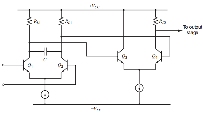
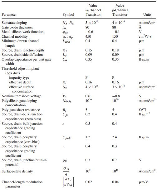
Table 2.4
Fantastic news! We've Found the answer you've been seeking!
Step by Step Answer:
From 669 From 118 with WL 3 WL 1 And I D1 I D...View the full answer

Answered By
Nazrin Ziad
I am a post graduate in Zoology with specialization in Entomology.I also have a Bachelor degree in Education.I posess more than 10 years of teaching as well as tutoring experience.I have done a project on histopathological analysis on alcohol treated liver of Albino Mice.
I can deal with every field under Biology from basic to advanced level.I can also guide you for your project works related to biological subjects other than tutoring.You can also seek my help for cracking competitive exams with biology as one of the subjects.
2+ Reviews
10+ Question Solved
Related Book For 
Analysis and Design of Analog Integrated Circuits
ISBN: 978-0470245996
5th edition
Authors: Paul R. Gray, Paul J. Hurst Stephen H. Lewis, Robert G. Meyer
Question Posted:
