

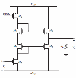
Design a CMOS output stage based on the circuit of Fig. 5.31 to deliver ±1 V before
Question:
Figure 5.31:
Fantastic news! We've Found the answer you've been seeking!
Step by Step Answer:
008 2 fn 650 mV 2 fp 750 mV Table 23 K n 127 AV K P 58 AV V tn 07 V V ...View the full answer

Answered By
Chiranjib Thakur
I have no tutoring experience yet, but I can share my skills and knowledge gained from my education and work experiences. I have been a CPA since 2012 with 6 years of work experience in internal auditing and 4 years of work experience in accounting at the supervisory level.
1+ Reviews
10+ Question Solved
Related Book For 
Analysis and Design of Analog Integrated Circuits
ISBN: 978-0470245996
5th edition
Authors: Paul R. Gray, Paul J. Hurst Stephen H. Lewis, Robert G. Meyer
Question Posted:
