

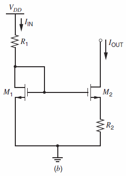
Design a MOS Widlar current source using the circuit shown in Fig. 4.31b to meet the following
Question:
(a) The input current should be 100 µA, and the output current should be 10 µA.
(b) Vov1 = 0.2 V.
(c) Transistor M2 must operate in the active region if the voltage from the drain of M2 to ground is at least 0.2 V.
(d) The output resistance should be 50 MΩ.
Ignore the body effect. Assume Ldrwn = 1 µm and Xd = Ld = 0. Use Table 2.4 for other parameters.
Fig. 4.31 (b):
Fantastic news! We've Found the answer you've been seeking!
Step by Step Answer:
Ignore BEX d L d 0 R o r o2 1 g m2 R 2 R o 5...View the full answer

Answered By
Gauri Hendre
I worked as EI educator for Eduphy India YT channel. I gave online tutorials to the students who were living in the villages and wanted to study much more and were preparing for NEET, TET. I gave tutions for topics in Biotechnology. I am currently working as a tutor on course hero for the biochemistry, microbiology, biology, cell biology, genetics subjects. I worked as a project intern in BAIF where did analysis on diseases mainly genetic disorders in the bovine. I worked as a trainee in serum institute of India and Vasantdada sugar institute. I am working as a writer on Quora partner program from 2019. I writing on the topics on social health issues including current COVID-19 pandemic, different concepts in science discipline. I learned foreign languages such as german and french upto A1 level. I attended different conferences in the science discipline and did trainings in cognitive skills and personality development skills from Lila Poonawalla foundation. I have been the member of Lila poonawalla foundation since 2017. Even I acquired the skills like Excel spreadsheet, MS Office, MS Powerpoint and Data entry.
4+ Reviews
10+ Question Solved
Related Book For 
Analysis and Design of Analog Integrated Circuits
ISBN: 978-0470245996
5th edition
Authors: Paul R. Gray, Paul J. Hurst Stephen H. Lewis, Robert G. Meyer
Question Posted:
