

For this problem, use the op amp in Fig. 12.23 and the CMFB scheme in Fig. 12.17.
Question:
Fig. 12.23:
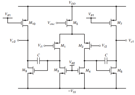
Fig. 12.16(b)
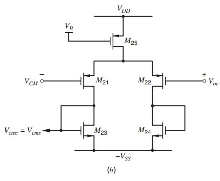
Figure 12.17:
(a) Design the CM-sense amplifier so that the total low-frequency gain acms0 = voc / vcms = ˆ’0.71, which is the same value as in the example in Section 12.6.1.
(b) With this CMFB circuit, what are the swing limits for each op-amp output voltage (Vo1 and Vo2)? Assume that the biasing current source in each source follower in Fig. 12.17 is implemented with a NMOS transistor, and the current-source and source-follower transistors operate with VGS = 0.8 V and Vov = 0.2V. For simplicity, assume VGS is constant and take γ = 0.
(c) What value of VCM gives the largest symmetric output swing?
(d) Verify that this CMFB circuit works correctly by running a SPICE simulation. Use the value of VCM from part (c).
Step by Step Answer:
a 071 Choose M23 to Match M5 WL 23 WL 5 25 Choose M25 to have an overdrive of 02 V I D25 ...View the full answer


Analysis and Design of Analog Integrated Circuits
ISBN: 978-0470245996
5th edition
Authors: Paul R. Gray, Paul J. Hurst Stephen H. Lewis, Robert G. Meyer
