

Replace the bipolar transistors in Fig. 7.40 with NMOS transistors. Repeat the calculations in Problem 7.21, using
Question:
Problem 7.21, using RS = 100 kΩ, RL = 3 kΩ, and the NMOS transistor model data in Problem 7.2, but use Cdb = 200 fF and Csb = 180 fF here. Take ID1 = 50 µA and ID2 = 1 mA.
Data from Prob. 7.21:
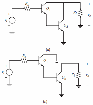
A Darlington stage and a common-collector€“common-emitter cascade are shown schematically in Fig. 7.40, where RS = 100 kΩ and RL = 3 kΩ.
(a) Calculate the low-frequency small-signal voltage gain Ï…o/Ï…i for each circuit.
(b) Use the zero-value time-constant method to calculate the ˆ’3-dB frequency of the gain of each circuit.
Fig. 7.40:
Fantastic news! We've Found the answer you've been seeking!
Step by Step Answer:
a In both cases 27 10 3 AV b For the Darlington stage C gs ...View the full answer

Answered By
Akash Goel
I am in the teaching field since 2008 when i was enrolled myself in chartered accountants course
Since then i have an experience of teaching of class XI, XII, BCOM, MCOM, MBA, CA CPT.
1+ Reviews
10+ Question Solved
Related Book For 
Analysis and Design of Analog Integrated Circuits
ISBN: 978-0470245996
5th edition
Authors: Paul R. Gray, Paul J. Hurst Stephen H. Lewis, Robert G. Meyer
Question Posted:
