

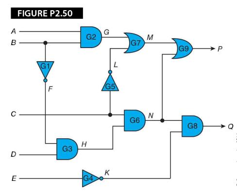
Consider the circuit in Figure P2.50. Assume that all gates are implemented in silicon by NANO gates,
Question:
Consider the circuit in Figure P2.50. Assume that all gates are implemented in silicon by NANO gates, NOR gates and inverters. Each NANO gate, NOR gate, or inverter has an internal delay of 0.4 ns. A logic transition at an input may cause a change at the output ( depending on other inputs and the circuit). The time for a transition at the input to appear as a corresponding transition at an output depends on the circuit path and the nature of the gates. What is the longest circuit path through this circuit? What is the worst case delay that a signal experiences going through the circuit?
Fantastic news! We've Found the answer you've been seeking!
Step by Step Answer:
The following diagram demonstrates all the paths t...View the full answer

Answered By
Aysha Ali
my name is ayesha ali. i have done my matriculation in science topics with a+ . then i got admission in the field of computer science and technology in punjab college, lahore. i have passed my final examination of college with a+ also. after that, i got admission in the biggest university of pakistan which is university of the punjab. i am studying business and information technology in my university. i always stand first in my class. i am very brilliant client. my experts always appreciate my work. my projects are very popular in my university because i always complete my work with extreme devotion. i have a great knowledge about all major science topics. science topics always remain my favorite topics. i am also a home expert. i teach many clients at my home ranging from pre-school level to university level. my clients always show excellent result. i am expert in writing essays, reports, speeches, researches and all type of projects. i also have a vast knowledge about business, marketing, cost accounting and finance. i am also expert in making presentations on powerpoint and microsoft word. if you need any sort of help in any topic, please dont hesitate to consult with me. i will provide you the best work at a very reasonable price. i am quality oriented and i have 5 year experience in the following field.
matriculation in science topics; inter in computer science; bachelors in business and information technology
_embed src=http://www.clocklink.com/clocks/0018-orange.swf?timezone=usa_albany& width=200 height=200 wmode=transparent type=application/x-shockwave-flash_
11+ Reviews
14+ Question Solved
Related Book For 
Computer Organization And Architecture Themes And Variations
ISBN: 9781111987046
1st Edition
Authors: Alan Clements
Question Posted:
