

Consider the following 8-bit bidirectional synchronous shift register with parallel load capability. The notation used to represent
Question:
CLR Asynchronous Clear, which overrides all other inputs
Q(7:0) 8-bit output
D(7:0) 8-bit input
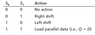
S0, S1mode control inputs
LSI serial input for left shift
RSI serial input for right shift
The mode control inputs work as follows:
(a) Write a Verilog module for this shift register.
(b) Draw a block diagram illustrating how two of these can be connected to form a 16-bit cyclic shift register, which is controlled by signals L and R. If L = 1 and R = 0, the 16-bit register is cycled left. If L = 0 and R = 1, the register is cycled right. If L = R = 1, the 16-bit register is loaded from X(15:0). If L = R = 0, the register is unchanged.
(c) Write a Verilog module for the module in part (b), using the module built in (a).
Fantastic news! We've Found the answer you've been seeking!
Step by Step Answer:
a module shift8Q D CLR CLK S0 ...View the full answer

Answered By
Collins Omondi
I have been an academic and content writer for at least 6 years, working on different academic fields including accounting, political science, technology, law, and nursing in addition to those earlier listed under my education background.
I have a Bachelor’s degree in Commerce (Accounting option), and vast knowledge in various academic fields Finance, Economics, Marketing, Management, Social Science, Women and Gender, Business law, and Statistics among others.
4+ Reviews
16+ Question Solved
Related Book For 

Digital Systems Design Using Verilog
ISBN: 978-1285051079
1st edition
Authors: Charles Roth, Lizy K. John, Byeong Kil Lee
Question Posted:
