

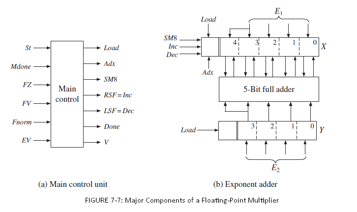
Redesign the floating-point multiplier in Figure 7. 7 using a common 5-bit full adder connected to a
Question:
(a) Redraw the block diagram, being sure to include the connections to the bus, and include all control signals.
(b) Draw a new SM chart for the new control.
(c) Write the Verilog description for the multiplier or specify the changes that need to be made to an existing description.
Fantastic news! We've Found the answer you've been seeking!
Step by Step Answer:
a b SM chart is similar to Figure 78 with added states for loading c define M B 0 module Prob711 CLK St Input Fout Eout V Done input CLK St input 3 0 ...View the full answer

Answered By
Rinki Devi
Professional, Experienced, and Expert tutor who will provide speedy and to-the-point solutions.
Hi there! Are you looking for a committed, reliable, and enthusiastic tutor? Well, teaching and learning are more of a second nature to me, having been raised by parents who are both teachers. I have done plenty of studying and lots of learning on many exciting and challenging topics. All these experiences have influenced my decision to take on the teaching role in various capacities. As a tutor, I am looking forward to getting to understand your needs and helping you achieve your academic goals. I'm highly flexible and contactable. I am available to work on short notice since I only prefer to work with very small and select groups of students.
I have been teaching students for 5 years now in different subjects and it's truly been one of the most rewarding experiences of my life. I have also done one-to-one tutoring with 100+ students and helped them achieve great subject knowledge.
2+ Reviews
10+ Question Solved
Related Book For 

Digital Systems Design Using Verilog
ISBN: 978-1285051079
1st edition
Authors: Charles Roth, Lizy K. John, Byeong Kil Lee
Question Posted:
