

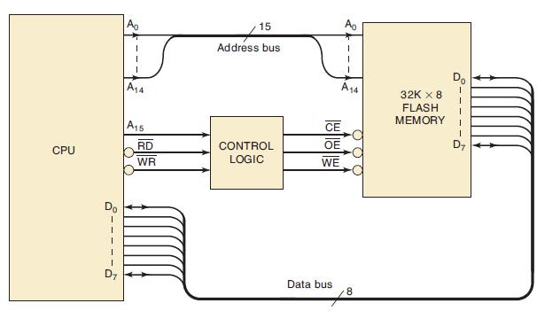
Figure 12-42 shows a small flash memory chip connected to a CPU over a data bus and
Question:
Figure 12-42 shows a small flash memory chip connected to a CPU over a data bus and an address bus. The CPU can write to or read from the flash memory array by sending the desired memory address and generating the appropriate control signals to the chip. The CPU asserts the R̅D̅ line when it has finished outputting a stable address and wants to read data from the memory device. The CPU asserts the W̅R̅ line after it has finished outputting a stable address and has placed the data to be stored on the data bus.
(a) What control logic is needed to allow this flash memory array to occupy addresses between 800016 and FFFF16?
(b) Which bus will carry the command codes from the CPU to the flash memory chip?
(c) What type of bus cycle will be executed to send control codes to the flash memory chip?
Figure 12-42
Step by Step Answer:
a To allow the flash memory array to occupy addresses between 800016 and FFFF16 the following contro...View the full answer


Digital Systems Principles And Application
ISBN: 9780134220130
12th Edition
Authors: Ronald Tocci, Neal Widmer, Gregory Moss
