

Refer to Problem 6-23. Modify the code of Figure 6-23 or Figure 6-24 to add an overflow
Question:
Refer to Problem 6-23. Modify the code of Figure 6-23 or Figure 6-24 to add an overflow output.
Figure 6-23
![123 10 10 5 6 7 8 9 10 11 4 b[7..0] 23 12 SUBDESIGN fig6_23 13 14 ( a [7..0] s [8..0] ) : INPUT; : INPUT; :](https://dsd5zvtm8ll6.cloudfront.net/images/question_images/1699/8/7/3/030655201068e0a21699873030153.jpg)
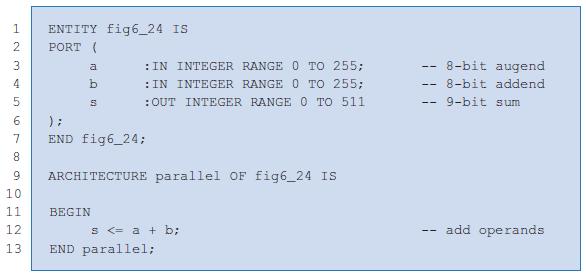
Figure 6-24
Data from Problem 6-23
In the adder and subtractor circuits discussed in this chapter, we gave no consideration to the possibility of overflow. Overflow occurs when the two numbers being added or subtracted produce a result that contains more bits than the capacity of the accumulator. For example, using four-bit registers, including a sign bit, numbers ranging from +7 to –8 (in 2’s complement) can be stored. Therefore, if the result of an addition or subtraction exceeds +7 or –8, we would say that an overflow has occurred. When an overflow occurs, the results are useless because they cannot be stored correctly in the accumulator register. To illustrate, add +5 101012 and +4 101002, which results in 1001. This 1001 would be interpreted incorrectly as a negative number because there is a 1 in the sign-bit position.
In computers and calculators, there are usually circuits that are used to detect an overflow condition. There are several ways to do this. One method that can be used for the adder that operates in the 2’s-complement system works as follows:
1. Examine the sign bits of the two numbers being added.
2. Examine the sign bit of the result.
3. Overflow occurs whenever the numbers being added are both positive and the sign bit of the result is 1 or when the numbers are both negative and the sign bit of the result is 0.
This method can be verified by trying several examples. Try the following cases: 112 5 + 4; 122 – 4 + 1–62; (3) 3 + 2. Cases 1 and 2 will produce an overflow, and case 3 will not. Thus, by examining the sign bits, one can design a logic circuit that will produce a 1 output whenever the overflow condition occurs. Design this overflow circuit for the adder of Figure 6-10.
Figure 6-10
Step by Step Answer:


Digital Systems Principles And Application
ISBN: 9780134220130
12th Edition
Authors: Ronald Tocci, Neal Widmer, Gregory Moss
