Optical waveguides can be fabricated in glass or crystal substrates by dopant diffusion as shown in Figure
Question:
Optical waveguides can be fabricated in glass or crystal substrates by dopant diffusion as shown in Figure P6.43. The process is similar to fabricating a transistor, but diffusion depths are deeper and since the diffusivities are small, an electric field is applied. Assuming a constant diffusivity, a constant applied electric field, the applicability of the Nernst-Einstein relationship, and diffusion depths small compared to substrate thickness:
a. Derive the following differential equation:
\[\frac{\partial c_{d}}{\partial t}=D \frac{\partial^{2} c_{d}}{\partial x^{2}}-\mu E \frac{\partial c_{d}}{\partial x}\]
b. What are the boundary conditions for this problem?
c. Show that the solution
\[c_{d}(x, t)=\frac{c_{d o}}{2}\left[\exp \left(\frac{\mu E x}{D}\right) \operatorname{erfc}\left(\frac{x+\mu E t}{\sqrt{4 D t}}\right)+\operatorname{erfc}\left(\frac{x-\mu E t}{\sqrt{4 D t}}\right)\right]\]
satisfies the differential equation and the boundary conditions.
d. In this operation, either diffusion can control the spread of dopant into the substrate or drift via the electric field can control it. What does the profile look like if drift within the field dominates?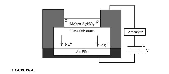
Step by Step Answer: