

Heat treatment is common in processing of semiconductor material. A 200-mm-diameter silicon wafer with thickness of 725
Question:
Heat treatment is common in processing of semiconductor material. A 200-mm-diameter silicon wafer with thickness of 725 mm is being heat treated in a vacuum chamber by infrared heater. The surrounding walls of the chamber have a uniform temperature of 310 K. The infrared heater provides an incident radiation flux of 200 kW/m2 on the upper surface of the wafer, and the emissivity and absorptivity of the wafer surface are 0.70. Using a pyrometer, the lower surface temperature of the wafer is measured to be 1000 K. Assuming there is no radiation exchange between the lower surface of the wafer and the surroundings, determine the upper surface temperature of the wafer.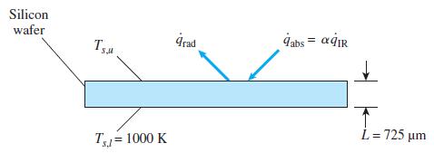
Step by Step Answer:
The upper surface temperature of the wafer is 975 K The heat transfer through the wafer can be calcu...View the full answer


Heat And Mass Transfer Fundamentals And Applications
ISBN: 9780073398181
5th Edition
Authors: Yunus Cengel, Afshin Ghajar
