

Question: 1. Assume VDD = 2.5V, Vss=0V. Assume the gate's load capacitance is 1 pF. a. Draw the schematic diagram for a standard CMOS gate
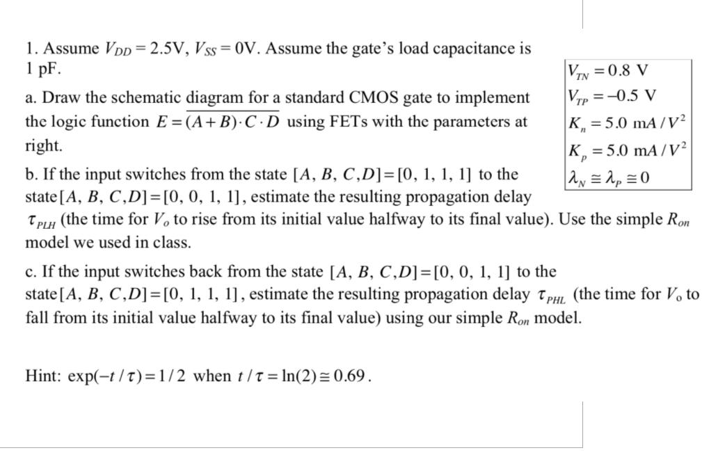
1. Assume VDD = 2.5V, Vss=0V. Assume the gate's load capacitance is 1 pF. a. Draw the schematic diagram for a standard CMOS gate to implement the logic function E = (A + B).C.D using FETs with the parameters at right. VIN=0.8 V VTP=-0.5 V K=5.0 mA/V K = 5.0 mA/V | = = 0 b. If the input switches from the state [A, B, C,D] = [0, 1, 1, 1] to the state [A, B, C,D] = [0, 0, 1, 1], estimate the resulting propagation delay TPLH (the time for V, to rise from its initial value halfway to its final value). Use the simple Ron model we used in class. c. If the input switches back from the state [A, B, C,D] = [0, 0, 1, 1] to the state [A, B, C,D] = [0, 1, 1, 1], estimate the resulting propagation delay TPHL (the time for Vo to fall from its initial value halfway to its final value) using our simple Ron model. Hint: exp(-t/t)=1/2 when t/t = ln(2) = 0.69.
Step by Step Solution
There are 3 Steps involved in it
Solution a b B K A T AB CD Pon m... View full answer

Get step-by-step solutions from verified subject matter experts