

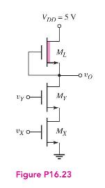
Consider a four-input NMOS NAND logic gate with a depletion load similar to the circuit in Figure
Question:
Consider a four-input NMOS NAND logic gate with a depletion load similar to the circuit in Figure P16.23. The bias voltage is \(V_{D D}=3.3 \mathrm{~V}\), and the threshold voltages are \(V_{T N D}=0.4 \mathrm{~V}\) and \(V_{T N L}=-0.6 \mathrm{~V}\). The logic 0 output voltage is to be \(0.10 \mathrm{~V}\).
(a) Using approximation methods, determine \(K_{D} / K_{L}\).
(b) The maximum power dissipation in the circuit is to be \(100 \mu \mathrm{W}\). Determine \((W / L)_{L}\) and \((W / L)_{D}\).
Fantastic news! We've Found the answer you've been seeking!
Step by Step Answer:

Answered By
Vivek Sheoran
I am clearing the doubts in minds of students related to math and chemistry from more than an year,
My students are always getting curious about science after being taught by me.
0 Reviews
10+ Question Solved
Related Book For 

Microelectronics Circuit Analysis And Design
ISBN: 9780071289474
4th Edition
Authors: Donald A. Neamen
Question Posted:
