

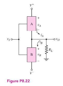
Consider an idealized class-B output stage shown in Figure P8.22. (The effective turn-on voltages of devices A
Question:
Consider an idealized class-B output stage shown in Figure P8.22. (The effective turn-on voltages of devices A and B are zero, and the effective "saturation" voltages of \(v_{A}\) and \(v_{B}\) are zero.) Assume \(V^{+}=5 \mathrm{~V}\) and \(V^{-}=\) \(-5 \mathrm{~V}\). Assume a symmetrical sine wave is produced at the output.
(a) What is the peak output voltage at maximum power conversion efficiency?
(b) What is the peak output voltage when each device dissipates the maximum power?
(c) If the maximum allowed power dissipation in each device is \(2 \mathrm{~W}\) and the output voltage is at its maximum value, what is the smaller permitted value of output load resistance?
Step by Step Answer:


Microelectronics Circuit Analysis And Design
ISBN: 9780071289474
4th Edition
Authors: Donald A. Neamen
