

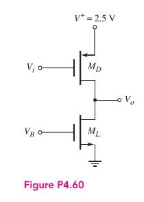
Consider the circuit in Figure P4.60. The transistor parameters are (V_{T P D}=-0.6 mathrm{~V}, quad V_{T N
Question:
Consider the circuit in Figure P4.60. The transistor parameters are \(V_{T P D}=-0.6 \mathrm{~V}, \quad V_{T N L}=0.4 \mathrm{~V}, \quad k_{n}^{\prime}=100 \mu \mathrm{A} / \mathrm{V}^{2}, \quad k_{p}^{\prime}=40 \mu \mathrm{A} / \mathrm{V}^{2}\), \(\lambda_{L}=0.02 \mathrm{~V}^{-1}, \lambda_{D}=0.04 \mathrm{~V}^{-1}\), and \((W / L)_{L}=10\).
(a) At the \(Q\)-point, the quiescent drain current is \(I_{D Q}=0.25 \mathrm{~mA}\). (i) Determine \((W / L)_{D}\) such that the small-signal voltage gain is \(A_{v}=V_{o} / V_{i}=-25\). (ii) What is the required value of \(V_{B}\) ? (iii) What is the value of \(V_{S G D Q}\) ?
(b) Repeat part (a) for \(I_{D Q}=0.1 \mathrm{~mA}\).
Fantastic news! We've Found the answer you've been seeking!
Step by Step Answer:

Answered By
Joseph Ogoma
I have been working as a tutor for the last five years. I always help students to learn and understand concepts that appears challenging to them. I am always available 24/7 and I am a flexible person with the ability to handle a wide range of subjects.
1+ Reviews
10+ Question Solved
Related Book For 

Microelectronics Circuit Analysis And Design
ISBN: 9780071289474
4th Edition
Authors: Donald A. Neamen
Question Posted:
