

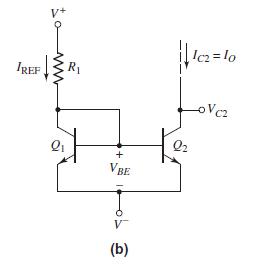
Consider the current source in Figure 10.2(b). The circuit is biased at (V^{+}=2.5 mathrm{~V}) and (V^{-}=-2.5 mathrm{~V}).
Question:
Consider the current source in Figure 10.2(b). The circuit is biased at \(V^{+}=2.5 \mathrm{~V}\) and \(V^{-}=-2.5 \mathrm{~V}\). The transistor parameters are \(\beta \cong \infty\), \(V_{A}=\infty\), and \(I_{S 2}=10^{-15} \mathrm{~A}\). The circuit is to be designed such that \(I_{O}=0.25 \mathrm{~mA}\) and the power dissipated in the circuit is no greater than \(1.8 \mathrm{~mW}\).
(a) Determine the maximum value of \(I_{\mathrm{REF}}\),
(b) the required value of \(I_{S 1}\), and
(c) the required value of \(R_{1}\).
Figure 10.2(b):-
Fantastic news! We've Found the answer you've been seeking!
Step by Step Answer:

Answered By
Rehab Rahim
I am well versed in communicating and teaching in areas of all business subjects. I have helped many students in different ways from answering answers to writing their academic papers.
1+ Reviews
10+ Question Solved
Related Book For 

Microelectronics Circuit Analysis And Design
ISBN: 9780071289474
4th Edition
Authors: Donald A. Neamen
Question Posted:
