

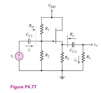
Consider the source-follower JFET amplifier in Figure P4.77 with transistor parameters (I_{D S S}=10 mathrm{~mA}, V_{P}=-5 mathrm{~V}),
Question:
Consider the source-follower JFET amplifier in Figure P4.77 with transistor parameters \(I_{D S S}=10 \mathrm{~mA}, V_{P}=-5 \mathrm{~V}\), and \(\lambda=0.01 \mathrm{~V}^{-1}\). Let \(V_{D D}=12 \mathrm{~V}\) and \(R_{L}=0.5 \mathrm{k} \Omega\).
(a) Design the circuit such that \(R_{\text {in }}=100 \mathrm{k} \Omega\), and the \(Q\)-point is at \(I_{D Q}=I_{D S S} / 2\) and \(V_{D S Q}=V_{D D} / 2\).
(b) Determine the resulting small-signal voltage gain \(A_{v}=v_{o} / v_{i}\) and the output resistance \(R_{o}\).
Fantastic news! We've Found the answer you've been seeking!
Step by Step Answer:
a RS12 mathrmk Ome...View the full answer

Answered By
Nimlord Kingori
2023 is my 7th year in academic writing, I have grown to be that tutor who will help raise your grade and better your GPA. At a fraction of the cost on other sites, I will work on your assignment by taking it as mine. I give it all the attention it deserves and ensures you get the grade that I promise. I am well versed in business-related subjects, information technology, Nursing, history, poetry, and statistics. Some software's that I have access to are SPSS and NVIVO. I kindly encourage you to try me; I may be all that you have been seeking, thank you.
360+ Reviews
1070+ Question Solved
Related Book For 

Microelectronics Circuit Analysis And Design
ISBN: 9780071289474
4th Edition
Authors: Donald A. Neamen
Question Posted:
