

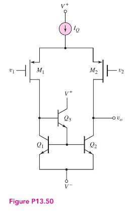
Design a BiCMOS amplifier that is complementary to the one in Figure P13.50 in that the input
Question:
Design a BiCMOS amplifier that is complementary to the one in Figure P13.50 in that the input devices are NMOS and the load transistors are pnp. Assume transistor parameters of \(V_{T N}=0.4 \mathrm{~V}, k_{n}^{\prime}=100 \mu \mathrm{A} / \mathrm{V}^{2}\), \(W / L=40, \lambda=0.02 \mathrm{~V}^{-1}, \beta=80\), and \(V_{A}=100 \mathrm{~V}\). Assume the bias current is \(I_{Q}=250 \mu \mathrm{A}\).
(a) Determine the small-signal parameters of the transistors.
(b) Find the small-signal differential voltage gain.
Fantastic news! We've Found the answer you've been seeking!
Step by Step Answer:

Answered By
Utsab mitra
I have the expertise to deliver these subjects to college and higher-level students. The services would involve only solving assignments, homework help, and others.
I have experience in delivering these subjects for the last 6 years on a freelancing basis in different companies around the globe. I am CMA certified and CGMA UK. I have professional experience of 18 years in the industry involved in the manufacturing company and IT implementation experience of over 12 years.
I have delivered this help to students effortlessly, which is essential to give the students a good grade in their studies.
2+ Reviews
10+ Question Solved
Related Book For 

Microelectronics Circuit Analysis And Design
ISBN: 9780071289474
4th Edition
Authors: Donald A. Neamen
Question Posted:
