

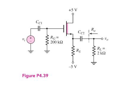
In the source-follower circuit in Figure P4.39 with a depletion NMOS transistor, the device parameters are: (V_{T
Question:
In the source-follower circuit in Figure P4.39 with a depletion NMOS transistor, the device parameters are: \(V_{T N}=-2 \mathrm{~V}, K_{n}=5 \mathrm{~mA} / \mathrm{V}^{2}\), and \(\lambda=0.01 \mathrm{~V}^{-1}\). Design the circuit such that \(I_{D Q}=5 \mathrm{~mA}\). Find the smallsignal voltage gain \(A_{v}=v_{o} / v_{i}\) and the output resistance \(R_{o}\).
Fantastic news! We've Found the answer you've been seeking!
Step by Step Answer:
RS12 ma...View the full answer

Answered By
Nazrin Ziad
I am a post graduate in Zoology with specialization in Entomology.I also have a Bachelor degree in Education.I posess more than 10 years of teaching as well as tutoring experience.I have done a project on histopathological analysis on alcohol treated liver of Albino Mice.
I can deal with every field under Biology from basic to advanced level.I can also guide you for your project works related to biological subjects other than tutoring.You can also seek my help for cracking competitive exams with biology as one of the subjects.
2+ Reviews
10+ Question Solved
Related Book For 

Microelectronics Circuit Analysis And Design
ISBN: 9780071289474
4th Edition
Authors: Donald A. Neamen
Question Posted:
