

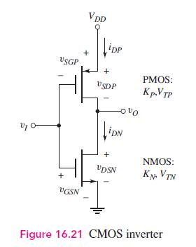
The CMOS inverter in Figure 16.21 is biased at (V_{D D}=3.3 mathrm{~V}). Let (K_{n}=K_{p}), (V_{T N}=0.5 mathrm{~V}),
Question:
The CMOS inverter in Figure 16.21 is biased at \(V_{D D}=3.3 \mathrm{~V}\). Let \(K_{n}=K_{p}\), \(V_{T N}=0.5 \mathrm{~V}\), and \(V_{T P}=-0.5 \mathrm{~V}\).
(a) Determine the two values of \(v_{I}\) and the corresponding values of \(v_{O}\) for which \(\left(d v_{O} / d v_{I}\right)=-1\) on the voltage transfer characteristics.
(b) Find the noise margins.
Fantastic news! We've Found the answer you've been seeking!
Step by Step Answer:

Answered By
Talha Talib
I am a member of IEEE society. As i am a student of electrical engineering badge 17 but beside of this i am also a tutor in unique academy. I teach calculus, communication skills, mechanics and economics. I am also a home tutor. My student Muhammad Salman Alvi is a brilliant A-level student and he performs very well in academics when i start to teach him. His weak point was mathematics but now he is performing well in mathematics. I am a scholarship holder in Fsc as i scored 1017 marks in metric out of 1100. Later on i got scholarship in Punjab Group of Colleges. I got 2nd position in robotics competition in 2018 as my project home automation select for the exhibition in Expocentre.
23+ Reviews
62+ Question Solved
Related Book For 

Microelectronics Circuit Analysis And Design
ISBN: 9780071289474
4th Edition
Authors: Donald A. Neamen
Question Posted:
