

The diff-amp configuration shown in Figure P11.7 is biased at (pm 3 mathrm{~V}). The maximum power dissipation
Question:
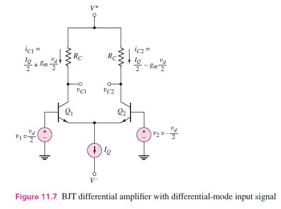
The diff-amp configuration shown in Figure P11.7 is biased at \(\pm 3 \mathrm{~V}\). The maximum power dissipation in the entire circuit is to be no more than \(1.2 \mathrm{~mW}\) when \(v_{1}=v_{2}=0\). The available transistors have parameters: \(\beta=120, V_{B E}\) (on) \(=0.7 \mathrm{~V}\), and \(V_{A}=\infty\). Design the circuit to produce the maximum possible differential-mode voltage gain, but such that the common-mode input voltage can be within the range \(-1 \leq v_{C M} \leq 1 \mathrm{~V}\) and the transistors are still biased in the forward-active region. What is the value of \(A_{d}\) ? What are the current and resistor values?
Fantastic news! We've Found the answer you've been seeking!
Step by Step Answer:

Answered By
Carly Cimino
As a tutor, my focus is to help communicate and break down difficult concepts in a way that allows students greater accessibility and comprehension to their course material. I love helping others develop a sense of personal confidence and curiosity, and I'm looking forward to the chance to interact and work with you professionally and better your academic grades.
12+ Reviews
21+ Question Solved
Related Book For 

Microelectronics Circuit Analysis And Design
ISBN: 9780071289474
4th Edition
Authors: Donald A. Neamen
Question Posted:
