

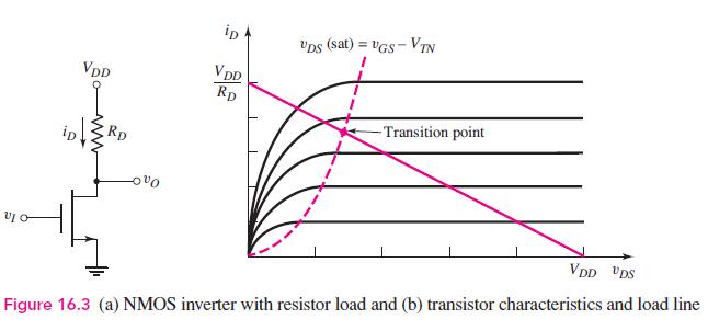
The inverter circuit in Figure 16.3 (a) is biased at (V_{D D}=3.3 mathrm{~V}). Assume the transistor conduction
Question:
The inverter circuit in Figure 16.3 (a) is biased at \(V_{D D}=3.3 \mathrm{~V}\). Assume the transistor conduction parameter is \(K_{n}=50 \mu \mathrm{A} / \mathrm{V}^{2}\).
(a) Let \(R_{D}=100 \mathrm{k} \Omega\). (i) Determine the transition point. (ii) Determine \(v_{O}\) for \(v_{I}=3.3 \mathrm{~V}\).
(b) Repeat part (a) for \(R_{D}=30 \mathrm{k} \Omega\).
(c) Repeat part (a) for \(R_{D}=5 \mathrm{k} \Omega\).
Fantastic news! We've Found the answer you've been seeking!
Step by Step Answer:

Answered By
Muhammad Umair
I have done job as Embedded System Engineer for just four months but after it i have decided to open my own lab and to work on projects that i can launch my own product in market. I work on different softwares like Proteus, Mikroc to program Embedded Systems. My basic work is on Embedded Systems. I have skills in Autocad, Proteus, C++, C programming and i love to share these skills to other to enhance my knowledge too.
1+ Reviews
10+ Question Solved
Related Book For 

Microelectronics Circuit Analysis And Design
ISBN: 9780071289474
4th Edition
Authors: Donald A. Neamen
Question Posted:
