

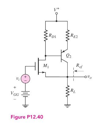
The parameters of the BiCMOS circuit in Figure P12.40 are (V^{+}=5 mathrm{~V}), (V_{G G}=2.5 mathrm{~V}, R_{D 1}=5
Question:
The parameters of the BiCMOS circuit in Figure P12.40 are \(V^{+}=5 \mathrm{~V}\), \(V_{G G}=2.5 \mathrm{~V}, R_{D 1}=5 \mathrm{k} \Omega, R_{E 2}=1.6 \mathrm{k} \Omega\), and \(R_{L}=1.2 \mathrm{k} \Omega\). The transistor parameters are \(K_{n}=1.5 \mathrm{~mA} / \mathrm{V}^{2}, V_{T N}=0.5 \mathrm{~V}, \lambda=0\) for \(M_{1}\) and \(h_{F E}=120, V_{E B}(\) on \()=0.7 \mathrm{~V}, V_{A}=\infty\) for \(Q_{2}\).
(a) Determine the quiescent values \(I_{D Q 1}\) and \(I_{C Q 2}\).
(b) Find the small-signal voltage gain \(A_{v}=v_{o} / v_{i}\).
(c) Determine the small-signal output resistance \(R_{o f}\).
Fantastic news! We've Found the answer you've been seeking!
Step by Step Answer:

Answered By
Fahmin Arakkal
Tutoring and Contributing expert question and answers to teachers and students.
Primarily oversees the Heat and Mass Transfer contents presented on websites and blogs.
Responsible for Creating, Editing, Updating all contents related Chemical Engineering in
latex language
8+ Reviews
22+ Question Solved
Related Book For 

Microelectronics Circuit Analysis And Design
ISBN: 9780071289474
4th Edition
Authors: Donald A. Neamen
Question Posted:
