

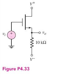
The source follower amplifier in Figure P4.33 is biased at (V^{+}=1.5 mathrm{~V}) and (V^{-}=-1.5 mathrm{~V}). The transistor
Question:
The source follower amplifier in Figure P4.33 is biased at \(V^{+}=1.5 \mathrm{~V}\) and \(V^{-}=-1.5 \mathrm{~V}\). The transistor parameters are \(V_{T N}=0.4 \mathrm{~V}\), \(k_{n}^{\prime}=100 \mu \mathrm{A} / \mathrm{V}^{2}, W / L=80\), and \(\lambda=0.02 \mathrm{~V}^{-1}\).
(a) The dc value of \(v_{O}\) is to be zero volts. What is the current \(I_{D Q}\) and the required value of \(V_{G S Q}\) ?
(b) Determine the small-signal voltage gain.
(c) Find the output resistance \(R_{o}\).
Fantastic news! We've Found the answer you've been seeking!
Step by Step Answer:
a ID Q015 ma...View the full answer

Answered By
JAPHETH KOGEI
Hi there. I'm here to assist you to score the highest marks on your assignments and homework. My areas of specialisation are:
Auditing, Financial Accounting, Macroeconomics, Monetary-economics, Business-administration, Advanced-accounting, Corporate Finance, Professional-accounting-ethics, Corporate governance, Financial-risk-analysis, Financial-budgeting, Corporate-social-responsibility, Statistics, Business management, logic, Critical thinking,
So, I look forward to helping you solve your academic problem.
I enjoy teaching and tutoring university and high school students. During my free time, I also read books on motivation, leadership, comedy, emotional intelligence, critical thinking, nature, human nature, innovation, persuasion, performance, negotiations, goals, power, time management, wealth, debates, sales, and finance. Additionally, I am a panellist on an FM radio program on Sunday mornings where we discuss current affairs.
I travel three times a year either to the USA, Europe and around Africa.
As a university student in the USA, I enjoyed interacting with people from different cultures and ethnic groups. Together with friends, we travelled widely in the USA and in Europe (UK, France, Denmark, Germany, Turkey, etc).
So, I look forward to tutoring you. I believe that it will be exciting to meet them.
2+ Reviews
10+ Question Solved
Related Book For 

Microelectronics Circuit Analysis And Design
ISBN: 9780071289474
4th Edition
Authors: Donald A. Neamen
Question Posted:
