

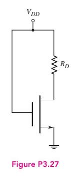
The transistor in the circuit in Figure P3.27 has parameters (V_{T N}=0.8 mathrm{~V}) and (K_{n}=0.25 mathrm{~mA} /
Question:
The transistor in the circuit in Figure P3.27 has parameters \(V_{T N}=0.8 \mathrm{~V}\) and \(K_{n}=0.25 \mathrm{~mA} / \mathrm{V}^{2}\). Sketch the load line and plot the \(Q\)-point for
(a) \(V_{D D}=4 \mathrm{~V}, R_{D}=1 \mathrm{k} \Omega\) and
(b) \(V_{D D}=5 \mathrm{~V}, R_{D}=3 \mathrm{k} \Omega\). What is the operating bias region for each condition?
Fantastic news! We've Found the answer you've been seeking!
Step by Step Answer:
a VD S188 mat...View the full answer

Answered By
Utsab mitra
I have the expertise to deliver these subjects to college and higher-level students. The services would involve only solving assignments, homework help, and others.
I have experience in delivering these subjects for the last 6 years on a freelancing basis in different companies around the globe. I am CMA certified and CGMA UK. I have professional experience of 18 years in the industry involved in the manufacturing company and IT implementation experience of over 12 years.
I have delivered this help to students effortlessly, which is essential to give the students a good grade in their studies.
2+ Reviews
10+ Question Solved
Related Book For 

Microelectronics Circuit Analysis And Design
ISBN: 9780071289474
4th Edition
Authors: Donald A. Neamen
Question Posted:
