

Calculate the small-signal voltage gain of a common-source amplifier with depletion load in Fig. 4.20, including both
Question:
Figure 4.20:
(a) Common-source amplifier with depletion-mode transistor load. (b) dc transfer characteristic.
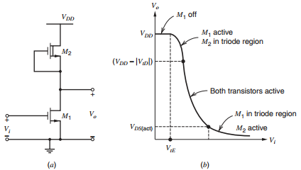
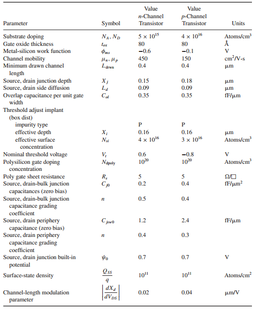
Table 2.4:
Fantastic news! We've Found the answer you've been seeking!
Step by Step Answer:
From 1140 C ox 39 886 10 14 80 10 8 43 10 7 Fcm 2 r ...View the full answer

Answered By
Moses mwangi
With prior writing experience, be sure that I will give a great grade, If not an A+, it will be something close to this. My reviews speaks it all, Try me!!
78+ Reviews
157+ Question Solved
Related Book For 
Analysis and Design of Analog Integrated Circuits
ISBN: 978-0470245996
5th edition
Authors: Paul R. Gray, Paul J. Hurst Stephen H. Lewis, Robert G. Meyer
Question Posted:
