

Design the MOS peaking current source in Fig. 4.34 so that I OUT = 0.1 µA. (a)
Question:
(a) First, let IIN = 1 µA and find the required value of R.
(b) Second, let R = 10 kΩ and find the required IIN.
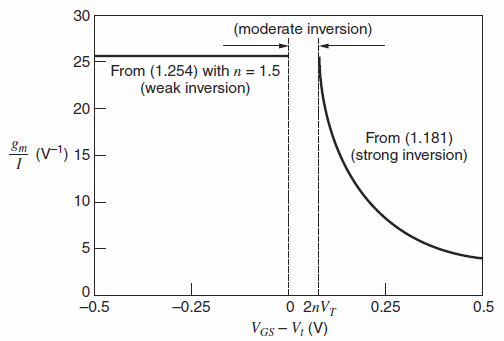
In both cases, assume that both transistors are identical and operate in weak inversion with It = 0.1 µA and n = 1.5. Also, find the minimum W/L in both cases, assuming that VGS ˆ’ Vt < 0 is required to operate a transistor in weak inversion as shown in Fig. 1.45.
Fig. 4.34:
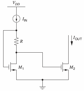
Fig. 1.45:
Fantastic news! We've Found the answer you've been seeking!
Step by Step Answer:
a I OUT 01 A when I 1N 1 A To keep tra...View the full answer

Answered By
Poonit Rathore
I have professional working experience of more than 4 years in a CA Firm.I have also teaching experience in commerce subject.
0 Reviews
10+ Question Solved
Related Book For 
Analysis and Design of Analog Integrated Circuits
ISBN: 978-0470245996
5th edition
Authors: Paul R. Gray, Paul J. Hurst Stephen H. Lewis, Robert G. Meyer
Question Posted:
