

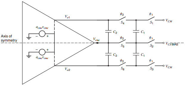
In the switched-capacitor CMFB scheme in Fig. 12.21, C 1 = 0.1 pF and C 2 =
Question:
(a) With VCSBIAS = ˆ’1 V, VOC = VCM = 0.5 V. If VCSBIAS changes to ˆ’1.1 V, what is the new value of VOC? Assume |acmc| >> 1.
(b) Ignoring all capacitors except C1 and C2, what are the CM and DM output load capacitors when the Ï•1 switches are on and the Ï•2 switches are off?
(c) Repeat (b) when the Ï•2 switches are on and the Ï•1 switches are off.
Fig. 12.21:
Fantastic news! We've Found the answer you've been seeking!
Step by Step Answer:
a V CM V OC V CBIAS V CMC 05 05 1 V ...View the full answer

Answered By
Robert Mwendwa Nzinga
I am a professional accountant with diverse skills in different fields. I am a great academic writer and article writer. I also possess skills in website development and app development. I have over the years amassed skills in project writing, business planning, human resource administration and tutoring in all business related courses.
187+ Reviews
378+ Question Solved
Related Book For 
Analysis and Design of Analog Integrated Circuits
ISBN: 978-0470245996
5th edition
Authors: Paul R. Gray, Paul J. Hurst Stephen H. Lewis, Robert G. Meyer
Question Posted:
