

In the fabrication of a p-type semiconductor, elemental boron is diffused a small distance into a solid
Question:
a. At what temperature must the boron-doping process be operated? It is known that the temperature dependence of the diffusion coefficient of boron (A) in silicon (B) is given by
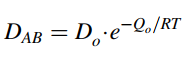
where Do = 0.0 19 cm2/s and Qo = 2.74 · 105 J/gmole for elemental boron in solid silicon. The thermodynamic con stant R = 8.314 J/gmole · K.
b. What is the flux of boron atoms at the silicon wafer surface at 10 min vs. 30 mm?
Fantastic news! We've Found the answer you've been seeking!
Step by Step Answer:
a Determine temperature T USS diffusion in semiinfinite med...View the full answer

Answered By
ANDREW KIPRUTO
Academic Writing Expert
I have over 7 years of research and application experience. I am trained and licensed to provide expertise in IT information, computer sciences related topics and other units like chemistry, Business, law, biology, biochemistry, and genetics. I'm a network and IT admin with +8 years of experience in all kind of environments.
I can help you in the following areas:
Networking
- Ethernet, Wireless Airmax and 802.11, fiber networks on GPON/GEPON and WDM
- Protocols and IP Services: VLANs, LACP, ACLs, VPNs, OSPF, BGP, RADIUS, PPPoE, DNS, Proxies, SNMP
- Vendors: MikroTik, Ubiquiti, Cisco, Juniper, HP, Dell, DrayTek, SMC, Zyxel, Furukawa Electric, and many more
- Monitoring Systems: PRTG, Zabbix, Whatsup Gold, TheDude, RRDtoo
Always available for new projects! Contact me for any inquiries
1+ Reviews
10+ Question Solved
Related Book For 

Fundamentals Of Momentum Heat And Mass Transfer
ISBN: 9781118947463
6th Edition
Authors: James Welty, Gregory L. Rorrer, David G. Foster
Question Posted:
