The Moss-Burstein Shift in Absorption Spectra The band filling or Moss-Burstein shift effect occurs in all heavily
Question:
The Moss-Burstein Shift in Absorption Spectra The “band filling” or Moss-Burstein shift effect occurs in all heavily doped three-dimensional semiconductors. It is a consequence of the fact that electrons are fermions, and therefore it is impossible (by the Pauli exclusion principle) to optically excite an electron into a same spin k-state, which is already occupied. In the case of strongly degenerate n+-doped sample, this has the effect of prohibiting any interband transition into electron states below the Fermi energy leading to an upward shift in the effective absorption edge,E0 g (see figure below). The Moss-Burstein shift (ΔE) is defined as the difference between the effective absorption edge and the energy gap (Eg) of the material, i.e., ΔE = E0 g - Eg.
(a) Calculate the Burstein shift in the absorption edge of a direct semiconductor with parabolic bands due to the heavy doping (n-type) at very low temperature (T≈0 K). The carrier concentration is ne. Neglect excitons. Note that the shift is not simply the Fermi energy of the electrons and involves the mass of both conduction and valence bands.
(b) Calculate the Moss-Burstein shift for the GaAs material doped with 1 x 10¹⁸ electrons/cm3. What should happen to the shape of the absorption edge? Assume m∗e = 0:067 m0 and m∗h = 0:45 m0 where m0is the electron rest mass.
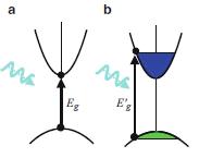
Allowed optical transitions in direct-gap semiconductors:
(a) undoped material, absorption threshold of Eg;
(b) n+-doped material, absorption threshold blue shifted to E0 g by the Moss-Burstein shift
Step by Step Answer:
a The MossBurstein shift in the absorption edge of a direct semiconductor with parabolic bands is g...View the full answer