

You are tasked with designing a 16 element micro-sensor array in a CMOS process. Because of space
Question:
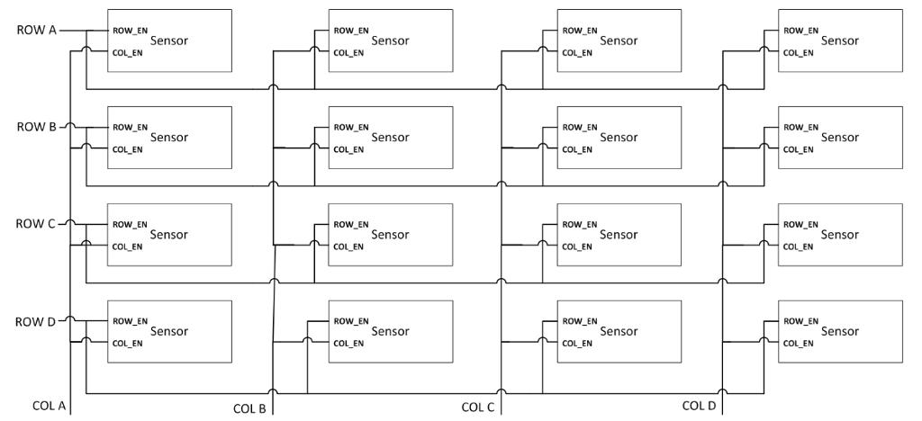
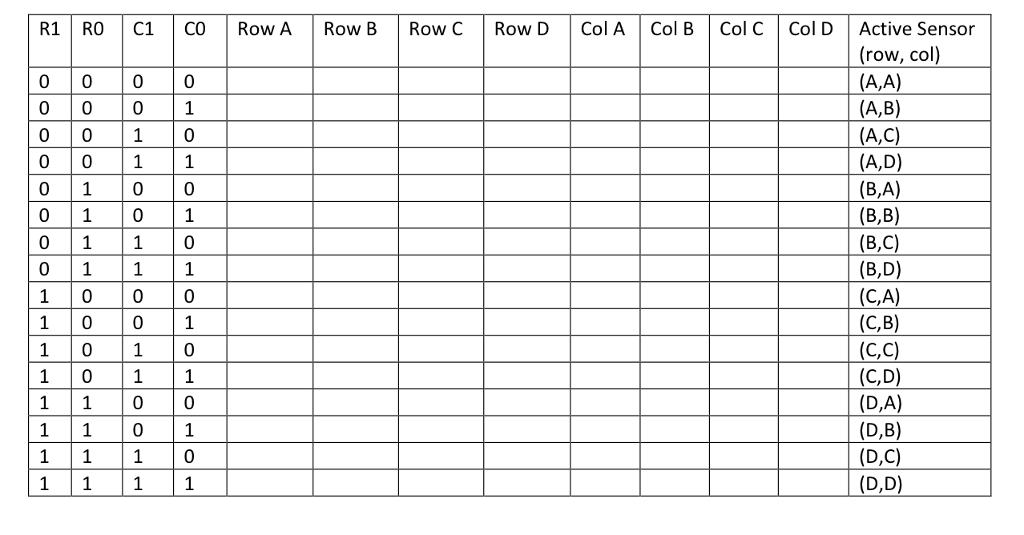
You are tasked with designing a 16 element micro-sensor array in a CMOS process. Because of space constraints on the silicon die, it is advantageous in minimizing area to use arbinary addressing system to activate each array element. This way, only 2 external inputs: ‘1’ or ‘0’ (VDD or GND) is applied to the row bits (R1, R0), and 2 external inputs for the column bits (C1, C0) so that only 4 external connections are required to activate any of the 16 elements. This particular array has 4 rows and 4 columns. Each of these elements is activated and its sensory response measured when both its row and column enable inputs are logic ‘1’. Only one sensor is allowed to be active at once. Therefore, the array is configured as follows:
a) Fill out the table with the proper row and column enable signals (0’s and 1’s) for each (ROW, COL) designation
b) Draw the logic circuit that implements this system and show how it connects to the sensors, using TWO 2:4 decoders. You should have a row decoder and column decoder. It may be helpful to first rewrite the table from part (a) into TWO new, separate tables.
c) Suppose that this CMOS process only provides 2:1 multiplexers (no decoders). Please draw the circuit that implements the same function using only 2:1 multiplexers and inverters. ONLY need to show the row or column circuit.
d) Assume we are no longer restricted to 2:1 multiplexers. Implement the same function using only multiplexers, no additional gates (could use any variety of MUXes of valid input:output). Show the row or column circuit from part (c).
Expert Answer:


Analysis and Design of Analog Integrated Circuits
ISBN: 978-0470245996
5th edition
Authors: Paul R. Gray,? Paul J. Hurst Stephen H. Lewis,? Robert G. Meyer
