

Design a CMOS op amp based on the folded-cascode architecture of Fig. 6.28 using supply voltages of
Question:
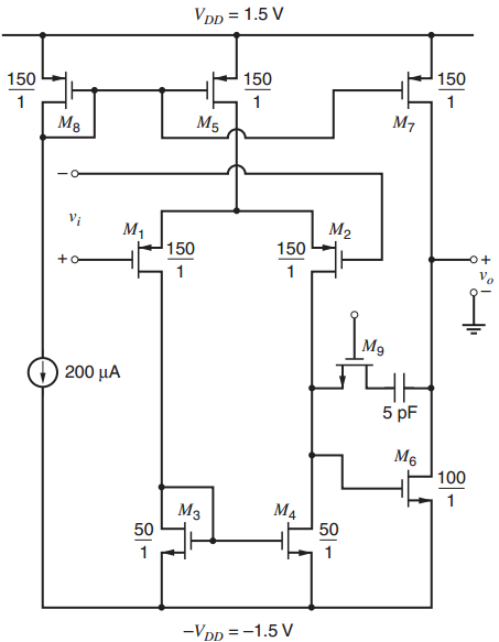
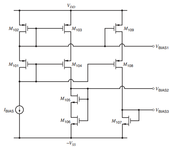
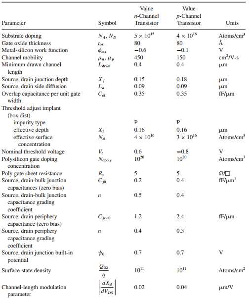
produces the bias voltagesVBIAS1, VBIAS2, and VBIAS3 based on IBIAS. The output current-drive capability is to be ± 100 μA, the output voltage-swing capability 1.5 Volts peak-peak, and the input common-mode range should extend from 0.5 V to the negative supply. Matching requirements dictate a minimum effective channel length of 1μm. To make the gain insensitive to small shifts in the operating point, design the circuit so that the magnitude of the drain-source voltage for each transistor operating in the active region exceeds the magnitude of its overdrive by at least 100 mV. Specify all device geometries and bias currents. The process is then-well process with parameters given in Table 2.4. Assume Xd =0 and γ = 0.25V ½ for both n- and p-channel transistors, but ignore the body effect in the hand calculations. Use SPICE to verify and refine your design as well as to determine the gain.
Figure 4.42
Table 2.4
Step by Step Answer:
For I 0max 100 A I D11 I D12 100 A Then half of I D11 should come from M 1 and the other half from M ...View the full answer


Analysis and Design of Analog Integrated Circuits
ISBN: 978-0470245996
5th edition
Authors: Paul R. Gray, Paul J. Hurst Stephen H. Lewis, Robert G. Meyer
