

For the CMOS operational amplifier shown in Fig. 9.60, calculate the open-loop voltage gain, unity gain bandwidth,
Question:
Fig. 9.60:
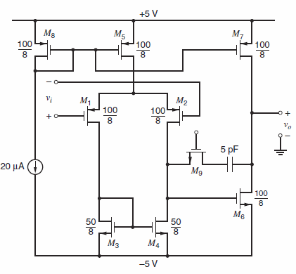
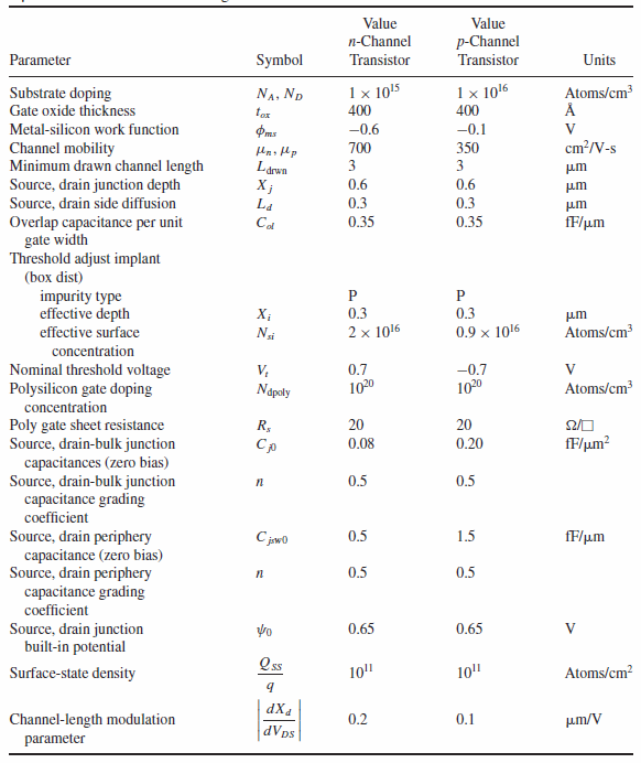
Table 2.1:
Fantastic news! We've Found the answer you've been seeking!
Step by Step Answer:
L eff L 2Ld Xd 8 203 1 64 I D 20 A for m g m 5 m 7 m 6 I D 10 ...View the full answer

Answered By
Asd fgh
sadasmdna,smdna,smdna,msdn,masdn,masnd,masnd,m asd.as,dmas,dma.,sd as.dmas.,dma.,s ma.,sdm.,as mda.,smd.,asmd.,asmd.,asmd.,asm
1+ Reviews
15+ Question Solved
Related Book For 
Analysis and Design of Analog Integrated Circuits
ISBN: 978-0470245996
5th edition
Authors: Paul R. Gray, Paul J. Hurst Stephen H. Lewis, Robert G. Meyer
Question Posted:
