

The feedback circuit in Fig. 12.58 is a switched-capacitor circuit during one clock phase. Assume the op
Question:
(a) Calculate the DM and CM output load capacitances, considering only the capacitances in the Fig. 12.58.
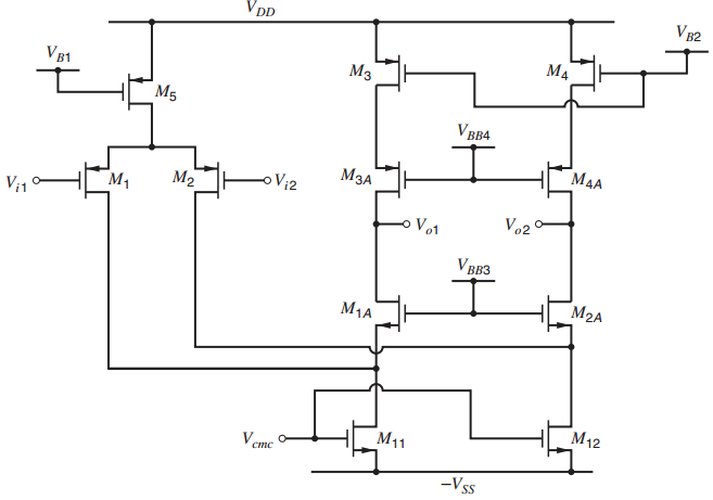
(b) If the op-amp bias currents are |ID3| = |ID4| = 100 µA and |ID5| = ID11 = ID12 = 200 µA, calculate the DM output slew rate dVod/dt.
(c) If all transistors have |Vov| = 0.15 V and VDD = VSS = 2 V, what is the maximum peak differential output swing? AssumeVBB3 and VBB4 are chosen to give maximum swing.
Fig. 12.52:
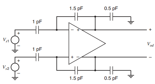
Fig. 12.31:
Fantastic news! We've Found the answer you've been seeking!
Step by Step Answer:
a b c V ss V ov11 V ov1A V o1 V ...View the full answer

Answered By
Atanu Ghosh
I have been teaching from the year 2014 to various type of student for competitive based examinations. Some of them are well placed now. I am very happy what I have done before. Even now I am continuing my job. I want to increase the fame.
So I will be very happy to solve some of your problems with all details and stepwise solutions.
0 Reviews
10+ Question Solved
Related Book For 
Analysis and Design of Analog Integrated Circuits
ISBN: 978-0470245996
5th edition
Authors: Paul R. Gray, Paul J. Hurst Stephen H. Lewis, Robert G. Meyer
Question Posted:
