

lw is the instruction with the longest latency on the CPU from Section 4.4. If we modified
Question:
lw is the instruction with the longest latency on the CPU from Section 4.4. If we modified lw and sw so that there was no offset (i.e., the address to be loaded from/stored to must be calculated and placed in rs before calling lw/sw), then no instruction would use both the ALU and Data memory. This would allow us to reduce the clock cycle time.
However, it would also increase the number of instructions, because many ld and sd instructions would need to be replaced with lw/add or sw/add combinations.
1. What would the new clock cycle time be?
2. Would a program with the instruction mix presented in Exercise 4.7 run faster or slower on this new CPU? By how much? (For simplicity, assume every lw and sw instruction is replaced with a sequence of two instructions.)
3. What is the primary factor that influences whether a program will run faster or slower on the new CPU?
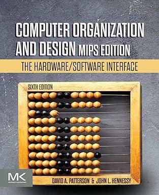
4. Do you consider the original CPU (as shown in Figure 4.21) a better overall design; or do you consider the new CPU a better overall design? Why?
Data from Exercise 4.7
Problems in this exercise assume that the logic blocks used to implement a processor’s datapath have the following latencies:
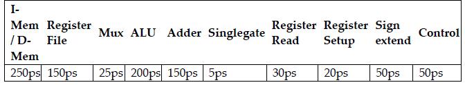
“Register read” is the time needed after the rising clock edge for the new register value to appear on the output. This value applies to the PC only. “Register setup” is the amount of time a register’s data input must be stable before the rising edge of the clock. This value applies to both the PC and Register File.
Figure 4.21
![PC Add Read address Instruction (31-01 Instruction [31-26] Instruction [25-21] Instruction [20-16]](https://dsd5zvtm8ll6.cloudfront.net/images/question_images/1703/7/6/8/476658d719c50eb01703768474996.jpg)
Step by Step Answer:
To answer these questions we need to consider the latencies of the components in the CPU and how changing the lw load word and sw store word instructions to require precalculated addresses affects the ...View the full answer


Computer Organization And Design MIPS Edition The Hardware/Software Interface
ISBN: 9780128201091
6th Edition
Authors: David A. Patterson, John L. Hennessy
