

For the following SM chart, (a) Draw a timing chart that shows the clock, the state (S
Question:
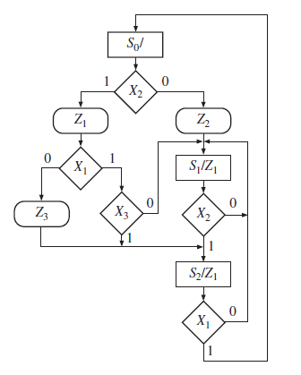
(a) Draw a timing chart that shows the clock, the state (S0, S1, or S2), the inputs (X1, X2, and X3), and the outputs. The input sequence is X1 X2 X3 = 011, 101,111,010,110,101,001. Assume that all state changes occur on the rising edge of the clock and the inputs change between clock pulses.
(b) Use the state assignment S0: AB = 00; S1: AB = 01; S2: AB = 10. Derive the next-state and output equations by tracing link paths. Simplify these equations using the don€™t care state (AB = 11).
(c) Realize the chart using a PLA and D flip-flops. Give the PLA table (state transition table).
(d) If a ROM is used instead of a PLA, what size ROM is required? Give the first five rows of the ROM table. Assume a naïve ROM method is used (i.e., a full look-up table).
Step by Step Answer:
a b A ABX 2 ABX 2 X 1 X 3 AB BX 2 AX 2 X 1 X 3 B ...View the full answer


Digital Systems Design Using Verilog
ISBN: 978-1285051079
1st edition
Authors: Charles Roth, Lizy K. John, Byeong Kil Lee
