

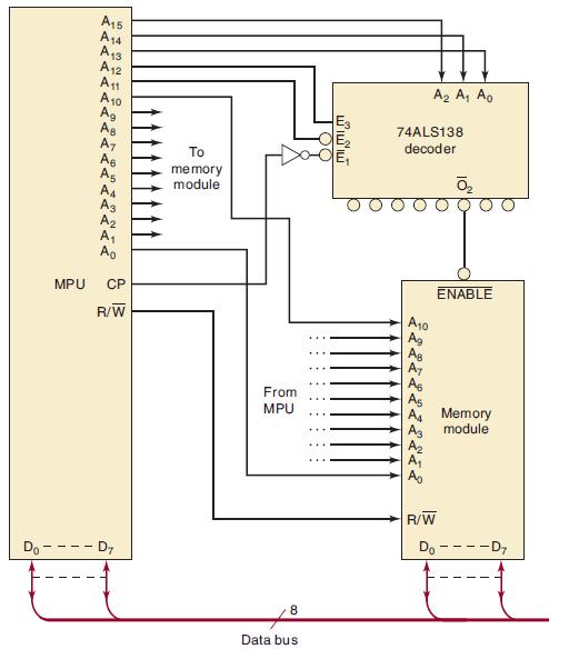
Figure 9-86 shows the basic circuitry to interface a microprocessor (MPU) to a memory module. The memory
Question:
Figure 9-86 shows the basic circuitry to interface a microprocessor (MPU) to a memory module. The memory module will contain one or more memory ICs (Chapter 12) that can either receive data from the MPU (a WRITE operation) or send data to the MPU (a READ operation). The data are transferred over the eight-line data bus. The MPU’s data lines and the memory’s I/O data lines are connected to this common bus. For now we will be concerned with how the MPU controls the selection of the memory module for a READ or WRITE operation. The steps involved are as follows:
1. The MPU places the memory address on its address output lines A15 to A0.
2. The MPU generates the R/W̅ signal to inform the memory module which operation is to be performed: R/W̅ = 1 for READ, R/W̅ = 0 for WRITE.
3. The upper five bits of the MPU address lines are decoded by the 74ALS138, which controls the ENABLE input of the memory module. This ENABLE input must be active in order for the memory module to do a READ or WRITE operation.
4. The other 11 address bits are connected to the memory module, which uses them to select the specific internal memory location being accessed by the MPU, provided that ENABLE is active. In order to read from or write into the memory module, the MPU must put the correct address on the address lines to enable the memory, and then pulse CP to the HIGH state.
(a) Determine which, if any, of these hexadecimal addresses will activate the memory module: 607F, 57FA, 5F00.
(b) Determine what range of hex addresses will activate the memory.
(c) Assume that a second identical memory module is added to the circuit with its address, R/W̅, and data I/O lines connected exactly the same as the first module except that its ENABLE input is tied to decoder output O̅4. What range of hex addresses will activate this second module?
(d) Is it possible for the MPU to read from or write to both modules at the same time? Explain.
Figure 9-86
Step by Step Answer:


Digital Systems Principles And Application
ISBN: 9780134220130
12th Edition
Authors: Ronald Tocci, Neal Widmer, Gregory Moss
