

Design a ternary full-adder circuit, using the approach described in Problem 3.25. Data From Problem 3.25 In
Question:
Design a ternary full-adder circuit, using the approach described in Problem 3.25.
Data From Problem 3.25
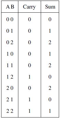
In a ternary number system there are three digits: 0, 1, and 2. Figure P3.3 defines a ternary half-adder. Design a circuit that implements this half-adder using binary-encoded signals, such that two bits are used for each ternary digit. Let A = a1a0, B = b1b0, and Sum = s1s0; Carry is just a binary signal. Use the following encoding: 00 = (0)3, 01 = (1)3, and 10 = (2)3. Minimize the cost of the circuit.
Fantastic news! We've Found the answer you've been seeking!
Step by Step Answer:
Full adder takes three inputs namely A B and C in Where ...View the full answer

Answered By
JAPHETH KOGEI
Hi there. I'm here to assist you to score the highest marks on your assignments and homework. My areas of specialisation are:
Auditing, Financial Accounting, Macroeconomics, Monetary-economics, Business-administration, Advanced-accounting, Corporate Finance, Professional-accounting-ethics, Corporate governance, Financial-risk-analysis, Financial-budgeting, Corporate-social-responsibility, Statistics, Business management, logic, Critical thinking,
So, I look forward to helping you solve your academic problem.
I enjoy teaching and tutoring university and high school students. During my free time, I also read books on motivation, leadership, comedy, emotional intelligence, critical thinking, nature, human nature, innovation, persuasion, performance, negotiations, goals, power, time management, wealth, debates, sales, and finance. Additionally, I am a panellist on an FM radio program on Sunday mornings where we discuss current affairs.
I travel three times a year either to the USA, Europe and around Africa.
As a university student in the USA, I enjoyed interacting with people from different cultures and ethnic groups. Together with friends, we travelled widely in the USA and in Europe (UK, France, Denmark, Germany, Turkey, etc).
So, I look forward to tutoring you. I believe that it will be exciting to meet them.
2+ Reviews
10+ Question Solved
Related Book For 

Fundamentals Of Digital Logic With Verilog Design
ISBN: 9780073380544
3rd Edition
Authors: Stephen Brown, Zvonko Vranesic
Question Posted:
