

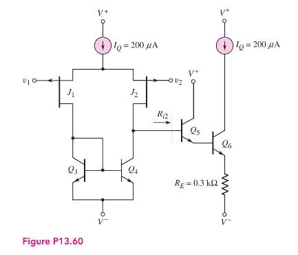
Consider the circuit in Figure P13.60. A JFET diff-amp input stage drives a bipolar Darlington second stage.
Question:
Consider the circuit in Figure P13.60. A JFET diff-amp input stage drives a bipolar Darlington second stage. The p-channel differential pair \(J_{1}\) and \(J_{2}\) are connected to the bipolar active load transistors \(Q_{3}\) and \(Q_{4}\). Assume JFET parameters of \(V_{P}=3 \mathrm{~V}, I_{D S S}=200 \mu \mathrm{A}\), and \(\lambda=0.02 \mathrm{~V}^{-1}\). The bipolar transistor parameters are \(\beta=100\) and \(V_{A}=50 \mathrm{~V}\).
(a) Determine the input resistance \(R_{i 2}\) to the second stage.
(b) Calculate the small-signal differentialmode voltage gain of the input stage. Compare this value to the 741 and CA3140 input stage results.
Fantastic news! We've Found the answer you've been seeking!
Step by Step Answer:

Answered By
Nyron Beeput
I am an active educator and professional tutor with substantial experience in Biology and General Science. The past two years I have been tutoring online intensively with high school and college students. I have been teaching for four years and this experience has helped me to hone skills such as patience, dedication and flexibility. I work at the pace of my students and ensure that they understand.
My method of using real life examples that my students can relate to has helped them grasp concepts more readily. I also help students learn how to apply their knowledge and they appreciate that very much.
1+ Reviews
10+ Question Solved
Related Book For 

Microelectronics Circuit Analysis And Design
ISBN: 9780071289474
4th Edition
Authors: Donald A. Neamen
Question Posted:
