

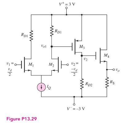
Consider the simple CMOS op-amp circuit in Figure P13.29 biased with (I_{Q}=200 mu mathrm{A}). The transistor parameters
Question:
Consider the simple CMOS op-amp circuit in Figure P13.29 biased with \(I_{Q}=200 \mu \mathrm{A}\). The transistor parameters are \(k_{n}^{\prime}=100 \mu \mathrm{A} / \mathrm{V}^{2}, k_{p}^{\prime}=\) \(40 \mu \mathrm{A} / \mathrm{V}^{2}, V_{T N}=0.4 \mathrm{~V}, V_{T P}=-0.4 \mathrm{~V}\), and \(\lambda_{n}=\lambda_{p}=0\). The transistor width-to-length ratios are \((W / L)_{1,2}=20,(W / L)_{3}=50\), and \((W / L)_{4}=40\).
(a) Design the circuit such that \(I_{D 3}=150 \mu \mathrm{A}, I_{D 4}=200 \mu \mathrm{A}\), and \(v_{o}=0\) for \(v_{1}=v_{2}=0\).
(b) Find the small-signal voltage gains (i) \(A_{d}=v_{o 1} / v_{d}\), (ii) \(A_{2}=v_{o 2} / v_{o 1}\), and (iii) \(A_{3}=v_{o} / v_{o 2}\).
(c) Determine the overall smallsignal voltage gain \(A=v_{o} / v_{d}\).
Step by Step Answer:


Microelectronics Circuit Analysis And Design
ISBN: 9780071289474
4th Edition
Authors: Donald A. Neamen
