

The BiCMOS folded cascode amplifier in Figure 13.20 is to be designed to provide a differential voltage
Question:
The BiCMOS folded cascode amplifier in Figure 13.20 is to be designed to provide a differential voltage gain of 25,000 . The maximum power dissipated in the circuit is to be limited to \(10 \mathrm{~mW}\). Assume MOS transistor parameters as described in Problem 13.43. The BJT parameters are \(\beta=120\) and \(V_{A}=80 \mathrm{~V}\).
Data From Problem 13.43:-
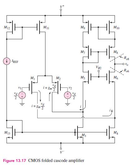
The CMOS folded cascode amplifier in Figure 13.17 is to be redesigned to provide a differential voltage gain of 10,000 . The biasing is the same as described in Problem 13.42. The transistor parameters are \(V_{T N}=0.5 \mathrm{~V}\), \(V_{T P}=-0.5 \mathrm{~V}, k_{n}^{\prime}=80 \mu \mathrm{A} / \mathrm{V}^{2}, k_{p}^{\prime}=35 \mu \mathrm{A} / \mathrm{V}^{2}, \lambda_{n}=0.015 \mathrm{~V}^{-1}\), and \(\lambda_{p}=0.02 \mathrm{~V}^{-1}\). Assume \((W / L)_{p}=2.2(W / L)_{n}\) where appropriate so that the electrical parameters of PMOS and NMOS devices are nearly identical.
Data From Problem 13.42:-
The CMOS folded cascode circuit in Figure 13.17 is biased at \(\pm 5 \mathrm{~V}\) and the reference current is \(I_{\mathrm{REF}}=50 \mu \mathrm{A}\). The transistor parameters are \(V_{T N}=0.5 \mathrm{~V}, V_{T P}=-0.5 \mathrm{~V}, K_{n}=K_{p}=0.5 \mathrm{~mA} / \mathrm{V}^{2}\), and \(\lambda_{n}=\lambda_{p}=\) \(0.015 \mathrm{~V}^{-1}\).
(a) Determine the small-signal differential voltage gain.
(b) Find the output resistance of the circuit.
(c) If the capacitance at the output node is \(C_{L}=5 \mathrm{pF}\), determine the unity-gain bandwidth of the amplifier.
Step by Step Answer:


Microelectronics Circuit Analysis And Design
ISBN: 9780071289474
4th Edition
Authors: Donald A. Neamen
