

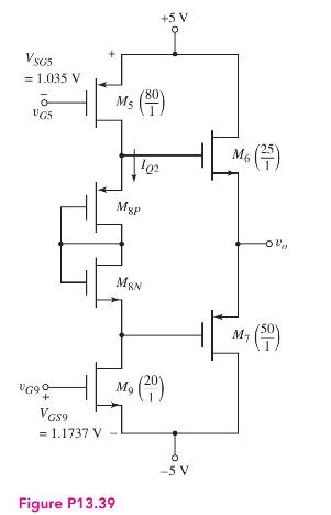
The circuit in Figure P13.39 is another form of an output stage for the CMOS op-amp shown
Question:
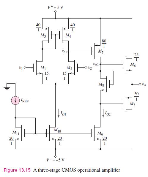
The circuit in Figure P13.39 is another form of an output stage for the CMOS op-amp shown in Figure 13.15. Assume the same transistor parameters as given in Example 13.10. The width-to-length values of some transistors are given and the applied gate-to-source voltages of \(M_{5}\) and \(M_{9}\) are shown.
(a) What is the bias current \(I_{Q 2}\) ?
(b) Determine the \(W / L\) ratios of \(M_{8 P}\) and \(M_{8 N}\) such that the quiescent currents in \(M_{6}\) and \(M_{7}\) are \(25 \mu \mathrm{A}\).
Fantastic news! We've Found the answer you've been seeking!
Step by Step Answer:

Answered By
Pharashram rai
i am highly creative, resourceful and dedicated freelancer an excellent record of successful classroom presentations and writing . I have more than 4 years experience in tutoring students especially by using my note making strategies and engineering field . Especially adept at teaching methods of maths and writing , and flexible teaching style with the willingness to work beyond the call of duty. Committed to ongoing professional development and spreading the knowledge within myself to the blooming ones to make them fly with .
65+ Reviews
270+ Question Solved
Related Book For 

Microelectronics Circuit Analysis And Design
ISBN: 9780071289474
4th Edition
Authors: Donald A. Neamen
Question Posted:
