

Design a 4-bit right-shift register using an FPGA with logic blocks as shown in Figure 6-1(a). When
Question:
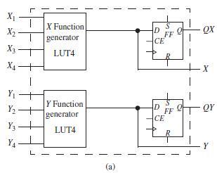
Design a 4-bit right-shift register using an FPGA with logic blocks as shown in Figure 6-1(a). When the register is clocked, the register loads if Ld = 1 and En = 1; it shifts right when Ld = 0 and En = 1; and nothing happens when En = 0. Si and So are the shift input and output of the register. D3-0and Q3-0are the parallel inputs and outputs, respectively. The next-state equation for the leftmost flip-flop is Q3+= En'Q3+ En (Ld D3+ Ld' Si).
(a) Give the next-state equations for the other three flip-flops.
(b) Determine the minimum number of Figure 6-1(a) logic blocks required to implement the shift register.
(c) For the left block, give the input connections and the internal paths on a copy of Figure 6-1(a). In addition, give the X and Y functions.
Figure 6-1(a)
Step by Step Answer:
a Q 2 EN Q 2 EN Ld D 2 Ld Q 3 Q 1 EN Q 1 EN Ld D 1 ...View the full answer


Digital Systems Design Using Verilog
ISBN: 978-1285051079
1st edition
Authors: Charles Roth, Lizy K. John, Byeong Kil Lee
