

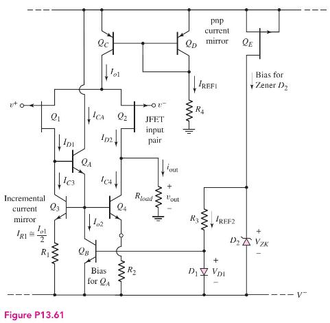
The BiFET diff-amp input stage in Figure P13.61 is biased at (I_{O 1}=1 mathrm{~mA}). The JFET parameters
Question:
The BiFET diff-amp input stage in Figure P13.61 is biased at \(I_{O 1}=1 \mathrm{~mA}\). The JFET parameters are \(V_{P}=4 \mathrm{~V}, I_{D S S}=1 \mathrm{~mA}\), and \(\lambda=0.02 \mathrm{~V}^{-1}\). The bipolar transistor parameters are \(\beta=200\) and \(V_{A}=100\) V.
(a) For \(R_{1}=R_{2}=500 \Omega\), determine the minimum load resistance \(R_{L}\) such that a differential-mode voltage gain of \(A_{d}=500\) is obtained in the input stage.
(b) If \(R_{L}=500 \mathrm{k} \Omega\), determine the range of resistance values \(R_{1}=R_{2}\) such that a differential-mode voltage gain of \(A_{d}=700\) is obtained in this input stage.
Fantastic news! We've Found the answer you've been seeking!
Step by Step Answer:

Answered By
Susan Juma
I'm available and reachable 24/7. I have high experience in helping students with their assignments, proposals, and dissertations. Most importantly, I'm a professional accountant and I can handle all kinds of accounting and finance problems.
15+ Reviews
45+ Question Solved
Related Book For 

Microelectronics Circuit Analysis And Design
ISBN: 9780071289474
4th Edition
Authors: Donald A. Neamen
Question Posted:
