

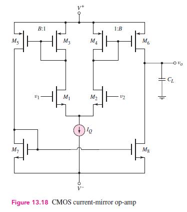
The CMOS current gain op-amp in Figure 13.18 is to be redesigned to provide a differential voltage
Question:
The CMOS current gain op-amp in Figure 13.18 is to be redesigned to provide a differential voltage gain of 400 . The transistor parameters are \(V_{T N}=0.5 \mathrm{~V}, V_{T P}=-0.5 \mathrm{~V}, k_{n}^{\prime}=80 \mu \mathrm{A} / \mathrm{V}^{2}, k_{p}^{\prime}=35 \mu \mathrm{A} / \mathrm{V}^{2}, \lambda_{n}=\) \(0.015 \mathrm{~V}^{-1}\), and \(\lambda_{p}=0.02 \mathrm{~V}^{-1}\). The bias current is to be \(I_{Q}=80 \mu \mathrm{A}\). Let \(B=2.5\).
(a) Design the basic amplifier to provide the specified voltage gain.
(b) Design a current source to provide the necessary bias current.
(c) Determine the unity-gain bandwidth if the capacitance at the output terminal is \(3 \mathrm{pF}\).
Step by Step Answer:


Microelectronics Circuit Analysis And Design
ISBN: 9780071289474
4th Edition
Authors: Donald A. Neamen
