

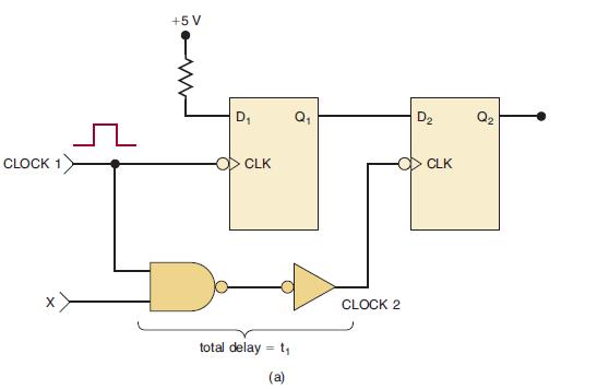
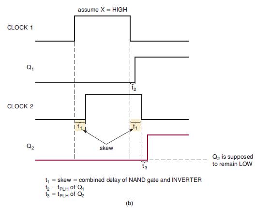
(a) Write an AHDL design file for the FF circuit shown in Figure 5-67. (b) Write a...
Question:
(a) Write an AHDL design file for the FF circuit shown in Figure 5-67.
(b) Write a VHDL design file for the FF circuit shown in Figure 5-67.
Figure 5-67
Fantastic news! We've Found the answer you've been seeking!
Step by Step Answer:

Answered By
Tamil Elakkiya Rajendran
I'm currently involved in the research in the field of Biothermodynamics, Metabolic pathway analysis and computational Biology. I always prefer to share my knowledge whatever I have learnt through my degree whenever time permits.
2+ Reviews
10+ Question Solved
Related Book For 

Digital Systems Principles And Application
ISBN: 9780134220130
12th Edition
Authors: Ronald Tocci, Neal Widmer, Gregory Moss
Question Posted:
