

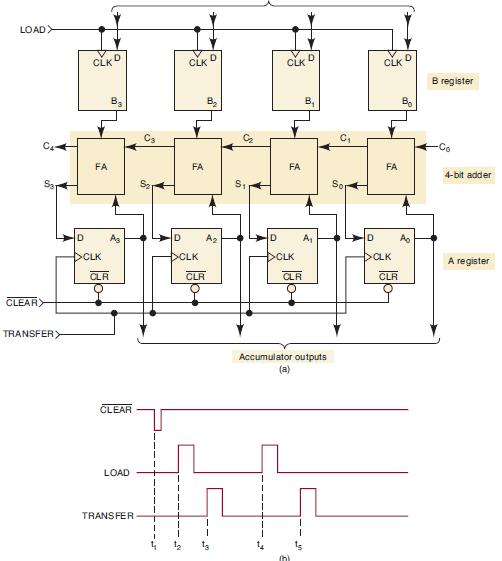
Design a look-ahead carry circuit for the adder of Figure 6-10 that generates the carry C 3
Question:
Design a look-ahead carry circuit for the adder of Figure 6-10 that generates the carry C3 to be fed to the FA of the MSB position based on the values of A0, B0, C0, A1, B1, A2, and B2. In other words, derive an expression for C3 in terms of A0, B0, C0, A1, B1, A2, and B2. (Begin by writing the expression for C1 in terms of A0, B0, and C0. Then write the expression for C2 in terms of A1, B1, and C1. Substitute the expression for C1 into the expression for C2. Then write the expression for C3 in terms of A2, B2, and C2. Substitute the expression for C2 into the expression for C3. Simplify the final expression for C3 and put it in sum-of-products form. Implement the circuit.)
Figure 6-10
Step by Step Answer:


Digital Systems Principles And Application
ISBN: 9780134220130
12th Edition
Authors: Ronald Tocci, Neal Widmer, Gregory Moss
