

Figure 11-21 shows how the ADC0804 is interfaced to a microcomputer. It shows three control signals, CS,
Question:
Figure 11-21 shows how the ADC0804 is interfaced to a microcomputer. It shows three control signals, C̅S̅, R̅D̅, and W̅R̅, that come from the microcomputer to the ADC. These signals are used to start each new A/D conversion and to read (transfer) the ADC data output into the microcomputer over the data bus.
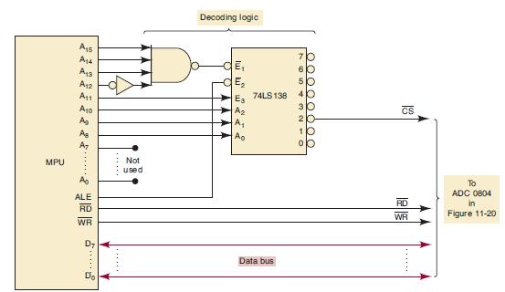
Figure 11-40 shows one way the address decoding logic could be implemented. The C̅S̅ signal that activates the ADC0804 is developed from the eight high-order address lines of the MPU address bus. Whenever the MPU wants to communicate with the ADC0804, it places the address of the ADC0804 onto the address bus, and the decoding logic drives the C̅S̅ signal LOW. Notice that in addition to the address lines, a timing and control signal (ALE) is connected to the E̅2 enable input. Whenever ALE is HIGH, it means that the address is potentially in transition, so the decoder should be disabled until ALE goes LOW (at which time the address will be valid and stable). This serves a purpose for timing but has no effect on the address of the ADC.
(a) Determine the address of the ADC0804.
(b) Modify the diagram of Figure 11-40 to place the ADC0804 at address E8XX hex.
(c) Modify the diagram of Figure 11-40 to place the ADC0804 at address FFXX hex.
Figure 11-40
Step by Step Answer:


Digital Systems Principles And Application
ISBN: 9780134220130
12th Edition
Authors: Ronald Tocci, Neal Widmer, Gregory Moss
