

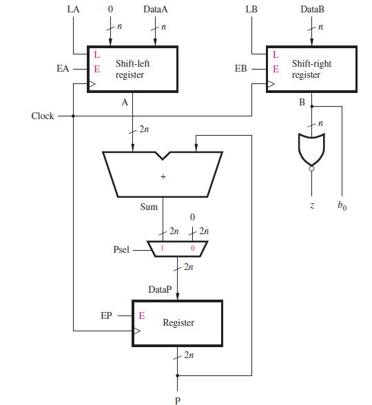
Figure 7.24 shows the data path circuit for the shift-and-add multiplier. It uses a shift register for
Question:
Figure 7.24 shows the data path circuit for the shift-and-add multiplier. It uses a shift register for B so that b0 can be used to decide whether or not A should be added to P. A different approach is to use a normal register to hold operand B and to use a counter and multiplexer to select bit bi in each stage of the multiplication operation.
(a) Show the ASM chart that uses a normal register for B, instead of a shift register.
(b) Show the data path circuit corresponding to part (a).
(c) Give the ASM chart for the control circuit corresponding to part (b).
(d) Give Verilog code that represents the multiplier circuit.
Fantastic news! We've Found the answer you've been seeking!
Step by Step Answer:
The image provided shows the data path circuit for a shiftandadd multiplier used in digital systems to perform multiplication of binary numbers Typically this method of multiplication involves shiftin...View the full answer

Answered By
Morgan Njeri
Very Versatile especially in expressing Ideas in writings.
Passionate on my technical knowledge delivery.
Able to multitask and able to perform under pressure by handling multiple challenges that require time sensitive solution.
Writting articles and video editing.
Revise written materials to meet personal standards and satisfy clients demand.
Help Online Students with their course work.
12+ Reviews
38+ Question Solved
Related Book For 

Fundamentals Of Digital Logic With Verilog Design
ISBN: 9780073380544
3rd Edition
Authors: Stephen Brown, Zvonko Vranesic
Question Posted:
